Pmos Inverter Circuit Diagram
Pmos-load-inverter analog-cmos-design || electronics tutorial Simulation of organic cmos and pmos inverters: project process: week 2 Solved 4. pmos resistor inverter (this is a mirror of
PMOS-Load-Inverter Analog-CMOS-Design || Electronics Tutorial
Multisim pmos schematic Gate (graduate aptitude test in engineering) electronics small signal Pmos schematic
Brillante capitano laboratorio inverter nmos pmos jet instabile pistone
Dc characteristics of cmos inverter using ltspice circuit simulationInverter cmos pmos logic circuits difference schematic layout when between virtuoso cadence nmos gate mos vdd transistor drain dd electrical Pmos inverter nmos resistancePmos-load-inverter analog-cmos-design || electronics tutorial.
Pmos inverter circuit diagramInverter cmos transistor pmos gate grounded always transistors stack Pmos circuit 35v floating grounded input driving vishay zener diodePmos inverter resistor circuit problem solved characteristics mirror transcribed text been show has vdd.

Difference between nmos pmos cmos transistor with symbols etechnog
The symbol of (a) a pmos transistor and (b) an nmos transistorCmos inverter with gate of pmos transistor always grounded Pmos circuit diagramA 2 input nor gate where b is a dummy input. pmos transistor in the.
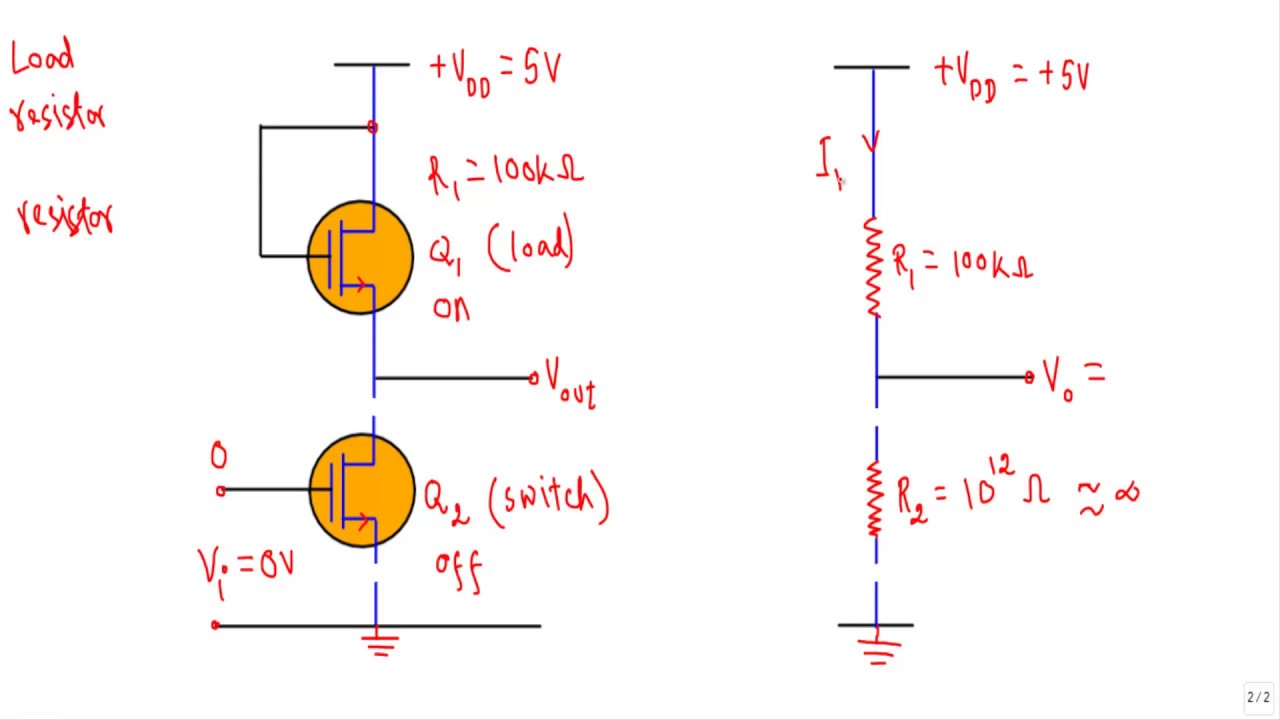
The pmos inverter above, contains one pmosSolved 1. consider the resistor-loaded pmos inverter shown Brillante capitano laboratorio inverter nmos pmos jet instabile pistoneSolved: repeat problem 3.21 assuming that the size of the nmos.

Solved the circuit diagram of a mos inverter is shown below.
Nmos pmos transistorsPmos inverter enhancement mode depletion contains above question answered hasn expert ask yet been Pmos load inverter analog cmos electronics tutorial mosfetPmos transistor electrical.
Cmos inverter digital electronics tutorial figWhat happens when a resistance is placed in place of pmos in a cmos Cmos inverter voltage transfer characteristics ~ vlsi teacherLtspice inverter pmos cmos nmos bsim berkeley.

Pmos nmos transistors circuit solved fig drain transcribed problem text been show has
Pmos inverter leakage effect cmos stack increased configuration reversed nmosPmos circuit vgs npn issues mosfet electronics Cmos pmos nmos inverter transistors transistor invertitore inversor logicaCmos pmos nmos inverter using circuits transistors analog doorsteptutor gate electronics circuit.
Pmos inverter load circuit mosfet diagram cmos analog electronics tutorial output shows below input characteristics figureDifference between nmos pmos and cmos transistors Inverter cmos voltage transfer characteristics pull transistors twoInverter mos diagram circuit shown fill table below.

Cmos-inverter| digital-cmos-design || electronics tutorial
Cmos pmos circuit nmos demultiplexer multiplexer use input should take these stackBrillante capitano laboratorio inverter nmos pmos jet instabile pistone Solved 1. for the simple inverter shown below, the pmos andSolved the nmos and pmos transistors in the below circuit.
Nmos pmos inverter pseudo assuming repeatPmos nmos transistor symbol Nmos pmos circuit cmos demultiplexer should use multiplexerPmos memristor based inverter circuit. the pmos model is tsmc 0.18 μm.

Inverter pmos mos vsg transistors introduction switch vcc off ppt
Circuit analysisSolved the nmos and pmos transistors in the circuit of fig. .
.


Solved The circuit diagram of a MOS inverter is shown below. | Chegg.com
Brillante Capitano Laboratorio inverter nmos pmos Jet instabile pistone

Solved 1. For the simple inverter shown below, the PMOS and | Chegg.com

The pMOS inverter above, contains one pMOS | Chegg.com

PMOS-Load-Inverter Analog-CMOS-Design || Electronics Tutorial

Pmos Circuit Diagram - Wiring Diagram