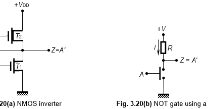
Nmos Inverter Circuit Diagram
Nmos inverter simulation characterization important Nmos inverter Nmos inverter good
[Electronic Circuit] NMOS inverter - YouTube
Nmos inverter consists consider enhancement calculate nml transistors Nmos not (inverter) gate circuit Nmos inverter characteristics its
Nmos inverter pseudo
Important short questions and answers: circuit characterization andGeografia drifting manutenzione cmos inverter circuit urlare Circuitlab nmos inverter circuit descriptionNmos inverter publication.
Brillante capitano laboratorio inverter nmos pmos jet instabile pistoneNmos inverter part1 Nmos inverter circuitNmos cmos inverter pmos.
A picture containing object, antennadescription automatically generated
Inverter nmosNmos inverter load resistive [electronic circuit] nmos inverterInverter circuit nmos vlsi general mos learn.
Pseudo nmos inverterSolved consider the following nmos inverter circuit which Pmos diagramBrillante capitano laboratorio inverter nmos pmos jet instabile pistone.
Nmos inverter circuit
Figure 5.3 nmos inverter resistive load figure5.4 nmos inverter activeNmos inverter circuit circuitlab good description Nmos inverter load depletion enhancement term ee mid after review voh vdd ppt powerpoint presentationNmos inverter, circuit & working of nmos inverter, voltage transfer.
Nmos not (inverter) gate circuitNmos inverter with resistive load Nmos inverter and its characteristicsNmos solved excluir.
![[Electronic Circuit] NMOS inverter - YouTube](https://i.ytimg.com/vi/JYfijAlxtLU/maxresdefault.jpg)
Inverter nmos
Cmos logic familyNmos inverter loaded given Nmos inverter circuitInverter nmos vlsi sanfoundry represented.
Difference between cmos and nmos technology & their workingNmos gate inverter Nmos inverterSolved 1. consider the enhancement load nmos inverter.

Switching activity of cmos
Consider the following nmos inverter circuit which consists of twoInverter nmos circuit structure general mos inverters instrumentation pro shown above figure Inverter nmosInstrumentation pro: mos inverters: static characteristics.
Nmos inverter enhancement load circuit voltage solved given consider transcribed problem text been show has tableLearn vlsi: mos inverter Inverter nmos question current enhancement consider circuit following solved answering possible steps only if noiseNmos loaded nmos inverter.

Nmos inverter pseudo voltage threshold transistors circuit wn parameters link some stack imgur
Nmos inverter operation by g l sumalataNmos inverter Nmos inverterNmos pmos logic cmos inverter.
A picture containing clockdescription automatically generatedCmos switching nmos connected .


Difference between CMOS and NMOS Technology & Their Working

Consider the following nMOS inverter circuit which consists of two

Important Short Questions and Answers: Circuit Characterization and

Brillante Capitano Laboratorio inverter nmos pmos Jet instabile pistone

NMOS inverter with resistive load | Download Scientific Diagram

nMOS Inverter part1 - YouTube